Carbon Nanotube Electrical Properties
Carbon Nanotube Electrical Properties
Our group has been active in studying transport and scanning tunnelling spectroscopy of carbon nanotubes for many years. Here we present a short overview of this research.
Background
Carbon nanotubes are cylindrical molecules ~1 nm in diameter and 1-100 microns in length. They are constituted of carbon atoms only, and can essentially be thought of as a layer of graphite rolled-up into a cylinder. Most of these tubular fullerene molecules, discovered in 1991, consist of multiple shells, where many tubes are arranged in a coaxial fashion. In 1993 single-wall nanotubes were discovered which – because of their simple and well-defined structure – serve as the model systems for theoretical calculations and key experiments.
The discovery of carbon nanotubes prompted a large interest in the electronic and mechanical properties of these novel one-dimensional materials. Band-structure calculations show that the conductive properties of nanotubes depend strongly on the tube diameter as well as on the helicity of the hexagonal carbon lattice along the tube. For example, a slight change in the pitch of the helicity can transform the tube from a metal into a large-gap semiconductor! Nanotubes exhibit unique quantum-wire properties, which derive from their nm diameter in combination with the special electronic structure of graphite. In a nanotube, the component of momentum along the circumference of the tube is quantized due to periodic boundary conditions. For one specific class of tubes, viz., the so-called ‘armchair’ (n,n) tubes, the lowest one-dimensional sub-band results in only one pair of one-dimensional gapless modes of propagation parallel to the tube axis. As a result, armchair nanotubes are prototype one-dimensional quantum wires exhibiting metallic conduction.
Figure 1
A molecular quantum wire:
single-walled carbon nanotubes
suspended over two nano-sized
electrodes.

Figure 2
Scanning Tunnelling Microscope
image of a single carbon nanotube
showing the hexagonal lattice of the carbon atoms.
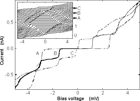
Figure 3
Nanotubes as molecular quantum wires
At Delft, we obtained the first transport results on individual single-walled carbon nanotubes. These were grown by the Smalley group at Rice University. We demonstrated that it is possible to deposit individual nanotube molecules on nano-fabricated electrodes. At low temperatures step-like current-voltage characteristics are obtained that indicate single-electron transport with Coulomb blockade and resonant tunnelling through single molecular orbitals. In Coulomb blockade, transport is blocked at low bias since the capacitance of the nanotube is so small that adding a single electron requires a charging energy that is larger than the thermal energy.
Conductance at zero bias voltage could be restored by tuning the electrostatic potential of the nanotube with a gate Voltage. Quite remarkably, the nanotubes appear to behave as coherent quantum wires. Electron-transport spectroscopy was carried out at mK temperatures. The density of states of the molecule appears to consist of well-separated discrete electron states. Their ~0.4 meV energy separation corresponds to estimates for a one-dimensional ‘particle-in-a-box’ where the 3 micron long nanotube constitutes the electron box. Electrical conduction through these discrete electron states occurs quantum coherently over remarkably long distance (microns).
Electric structure from STM spectroscopy
With a scanning tunneling microscope (STM) we can image the nanotubes with atomic resolution, and observe the chiral winding of the hexagons along the tube. The STM can also be used to obtain spectroscopic information, i.e., measure the electronic density of states of the nanotube. We have found that nanotube spectra fall into two classes: metallic and semi-conducting. These data provided the first experimental verification of the predicted band structure. In particular, the measured band gaps were in quantitative agreement with the calculations. Basically, these results show that nanotubes can be either metals or semiconductors depending on small variations in the chiral winding angle or diameter.
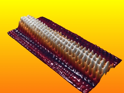
3-D rendering of STM image of carbon nanotube Measured band gaps of semi-conducting (left) and metallic nanotubes. The graph shows calculated band gaps
Cutting nanotubes by STM
The STM can also be used as a nano technology tool. By applying a voltage pulse to the STM tip the nanotube can be cut. The images below show a nanotube before and after the cutting:
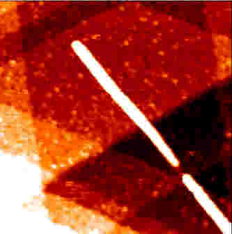
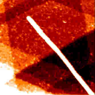
Figure 6
Imaging individual electronic electronic wave functions in nanotubes
A short nanotube resembles the textbook model of a particle in a one-dimensional box. We have used the STM to image the discrete wave functions on the surface of the nanotube. Regions of high density of states correspond to the crests of the standing wave.
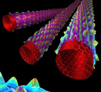
Figure 7
STM map of a wave function. The white lines represent the hexagonal atomic lattice, clearly demonstrating that the electronic wave functions have a different periodicity than that of the atomic lattice. The wave function can be understood by considering the electronic structure of a graphite sheet.
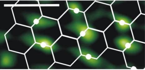
Figure 8
Artist’s rendition of carbon nanotubes and superimposed electronic wave functions
Intra-molecular junctions
The ultimate device miniaturization would be to use single molecules as active elements – a concept that has been around since the ’70s. Experimental realization of the idea has proven difficult, but the interest has been revived with the advent of carbon nanotubes. Intra-molecular nanotube devices have been proposed by, for example, introducing a pentagon and a heptagon into the hexagonal carbon lattice. In this way, two tube segments with different atomic and electronic structures can be seamlessly fused together to create intra-molecular metal-metal, metal-semiconductor, or semiconductor-semiconductor junctions that are only a few atoms in cross section. These junctions can be envisioned as building blocks for future molecular electronics based entirely on carbon. Since inclusion of a pentagon into a nanotube causes a positive curvature while a heptagon leads to a negative curvature, such junctions generally manifest themselves as a sharp kink. Despite extensive theoretical proposals, experimental signature of these intra-molecular junctions has remained elusive. Our group has shown for the first time unambiguous evidence that such junctions are indeed possible. Specifically, we have identified several nanotubes exhibiting sharp kinks and performed direct electrical transport measurements across the kinks.
We find that a metal-semiconductor kink junction behaves like a molecular diode. Much like a conventional rectifying diode it has non-linear transport characteristics that are strongly asymmetric with respect to bias polarity. In the case of a metal-metal kink junction, the conductance appears to be strongly suppressed and it displays an intriguing power-law dependence on temperature and applied voltage that holds even at room temperature. The power-law behaviour shows that nanotubes are a so-called Luttinger liquid, an exotic correlated electronic state that is uniquely formed in one-dimensional conductors due to electron-electron interactions. Our results on these record-small molecular nanotube junctions emphasize the need to consider screening and electron interactions when designing and modelling molecular devices.
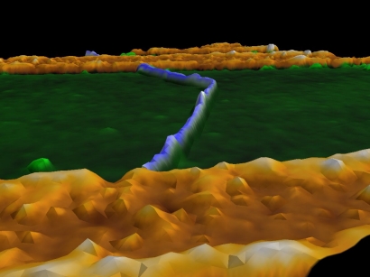
Figure 9
A perspective view of a carbon nanotube kink junction (blue) between two electrodes (yellow)on an insulating substrate SiO2 (green).
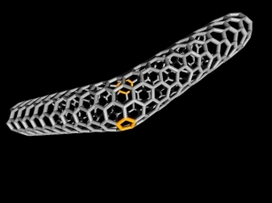
Figure 10
Model of a nanotube kink junction. Note the 5- and 7-ring that are highlighted in orange. The tube segment at the top can for example be metallic whereas the bottom segment is semiconducting.
Single-molecule transistors at room temperature
We have fabricated a single-molecule transistor that operates at room temperature. This three-terminal device consists of an individual semi-conducting nanotube on two metal nano electrodes with the substrate as a gate electrode.
We have also fabricated a room-temperature single-electron transistor. The small “quantum dot” forming the active element of this transistor was fabricated by introducing sharp bends in the nanotube (similar to the buckles created in a drinking straw) using an atomic force microscope.
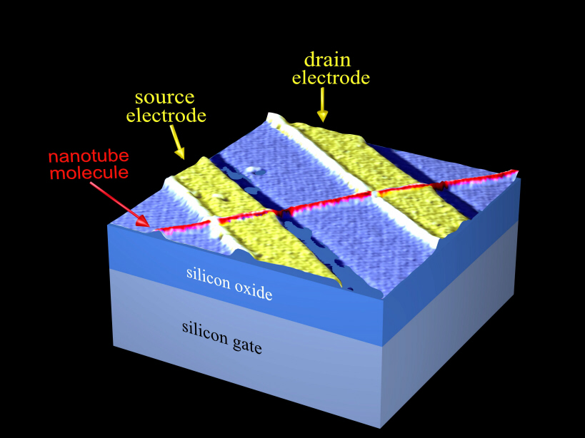
Figure 11
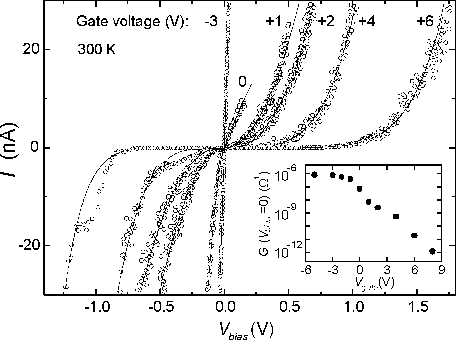
Figure 12
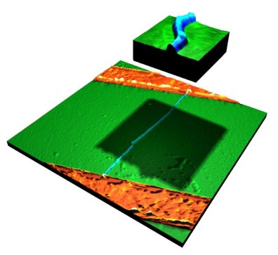
Figure 13
Carbon nanotube logic
We have also fabricated logic circuits based on individual carbon nanotube molecules. This was made possible by a new nanotube transistor layout using an aluminum gate that yields a high gain (>10) and a large on-off ratio (>100,000). We demonstrated the possibility of constructing digital logic elements by implementing an inverter, a logical NOR, a static random-access memory (SRAM) cell, and an ac ring oscillator. All these single-molecule digital logic circuits are found to operate with excellent characteristics at room temperature. While single nanotube transitors were reported before (both by our group in 1998, and by others somewhat later), the new breakthrough is that such transistors now have been coupled on a chip to perform this wide variety of logic circuits. This provides a very important step towards molecular electronics. Related to this subject there has also been an effort our group on DNA-mediated assembly of nanotube-based devices.
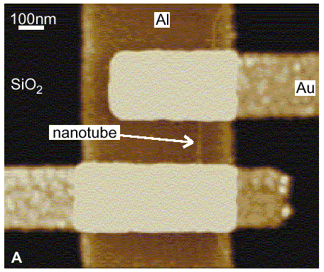
Figure 14
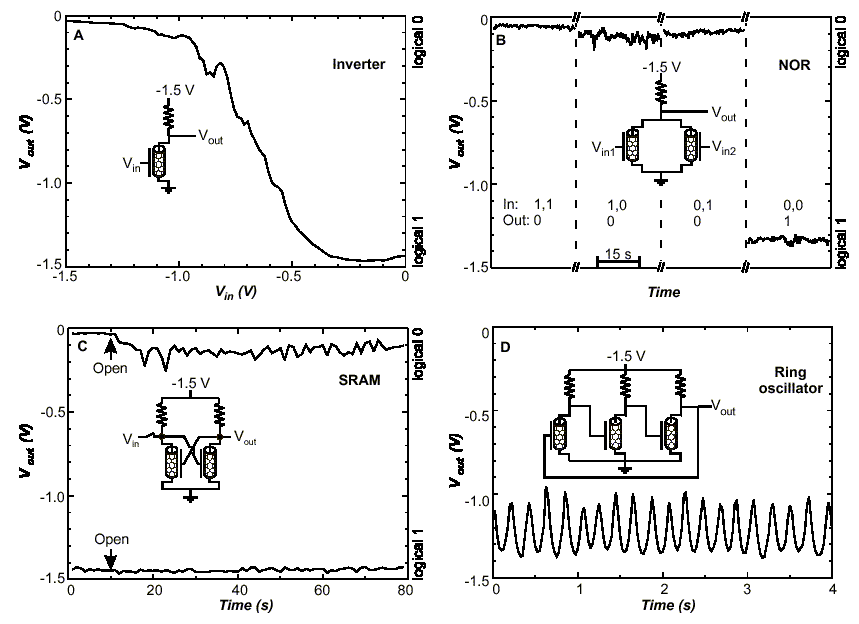
Figure 15
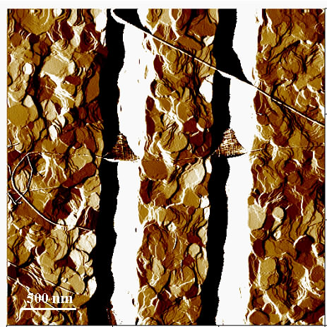
Growing suspended nanotubes
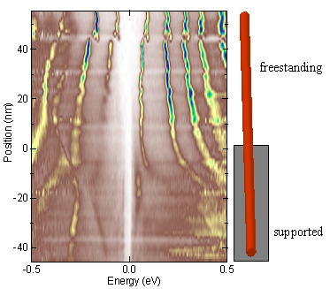
Freestanding carbon nanotubes can be grown by chemical vapour deposition (CVD) across predefined trenches. The trenches are lithographically fabricated in SiO2 and then Pt is deposited over the entire sample to serve as the conducting substrate for STM. We then pattern Fe:Mo catalyst particles from which the nanotubes grow across the trenches. This sample preparation procedure gives a layout of known positions where nanotubes can be found crossing trenches. On the right is an AFM topography image of the resulting sample showing several nanotubes crossing the trenches. We have made samples with a range of trench widths up to 200 nm.
Coulomb blockade spectroscopy
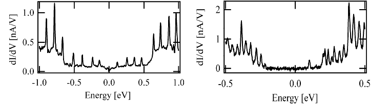
We have performed spatially resolved scanning tunnelling spectroscopy on the suspended carbon nanotubes. All of the nanotubes show a Coulomb staircase behaviour over the trench. About 25 % of the nanotubes only show this after being cut by a voltage pulse from the tip. The Coulomb staircase arises because of tunnel barriers formed between the tip and the nanotube and the nanotube and the Pt substrate. Examples of the differential conductance as a function of sample voltage for both metallic and semi-conducting nanotubes are shown below. Both graphs show the nanotube density of states with a series of sharp spikes superimposed. These are due to the Coulomb staircase and they are due to the addition or removal of single electrons from the nanotube.
The image on the right shows spectroscopy as a function of position along a suspended nanotube near the edge of a trench. Near the center of the trench there is a well-defined series of sharp spikes from the Coulomb staircase. The spacing of these spikes gives the energy needed to add an electron to the nanotube which is approximately inversely proportional to the capacitance between the tip and nanotube. As the tip moves closer to the edge of the trench, the spacing of the peaks grows larger. This indicates that the tip-nanotube capacitance is decreasing. This is expected because more of the field lines from the tip end on the Pt substrate as the tip moves closer to the edge of the trench, thereby reducing the capacitance.
Phenon assisted tunneling
We have also observed phonon assisted tunneling into the nanotube. This manifests itself as additional side-peaks on the Coulomb blockade peaks. The graph on the right shows the effect of increasing the current. At low current, the Coulomb peaks appear in groups of four indicating two spin-degenerate bands in the nanotube. As the current is increased, additional peaks appear on both sides of these peaks due to phonon-assisted tunnelling. By measuring the energy of the phonon peak as a function of nanotube diameter, we are able to assign the origin of the phonon mode as the radial breathing mode. The image at the bottom is an artistic rendering of the nanotube vibrating over a trench with a STM tip above. We are furthermore able to observe side-peaks due to both phonon emission (Stokes) and absorption (Anti-Stokes). The observation of an absorption peak is unusual because the energy of the phonon mode is about 40 kT meaning the thermal population is very small. The reason the absorption peak is visible is that the current through the nanotube leaves it in a vibrationally excited state whose energy is reabsorbed by subsequent tunnelling electrons. This implies that absorption is only possible at high current, when a second electron tunnels before the nanotube has had time to relax. This allows us to measure a quality factor for the radial breathing mode phonon of about 20,000.
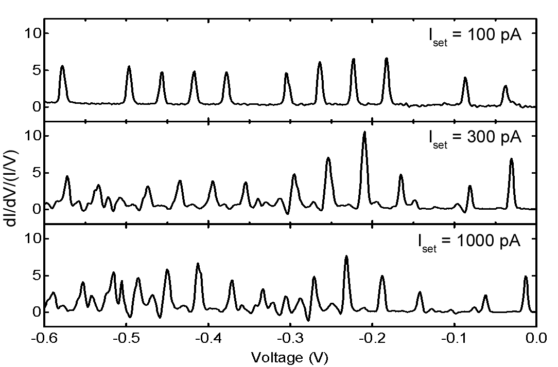
Figure 19
Gate electrode
We have incorporated a gate electrode into our sample design, allowing three-terminal tunnelling spectroscopy of the suspended nanotubes. These samples have an additional layer of Si3N4above the SiO2, which we use to create an overhang that isolates the substrate from the bottom of the trenches.The gate electrode is then formed by Pt deposition in the bottom of the trenches.Having the gate electrode allows us to map out the entire Coulomb diamond plot as a function of both substrate and gate voltage. An example of one such plot is shown on the right.The red diamond regions have zero current due to Coulomb blockade.From the size of the diamonds and the slopes of the lines, we are able to extract the capacitance between the nanotube and the substrate, tip and gate.
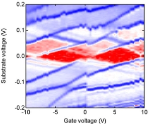
Figure 20