Graphene nanodevices
In recent years, 2D materials such as graphene have attracted much attention for a wide range of interesting transport and physical properties. At our lab, we pioneered the use of graphene nanopores for detection of DNA (see our paper G.F. Schneider et al., Nano Lett., 10, 3163–3167 (2010)). Due to their extreme thinness, they could theoretically provide maximal resolution. However, the noise levels in the ionic current are currently high and fabrication challenges remain. Ongoing projects in the lab are investigating new detection schemes through graphene tunneling mechanical breakjunctions as well as novel new graphene devices for studying single biomolecule transport of DNA.
Figure 1: Four concepts for DNA sequencing using graphene nanostructures. a) Detection of changes in the ionic current through a nanopore in a graphene membrane due to the passage of a DNA molecule. b) Modulations of a tunnelling current through a nanogap between two graphene electrodes due to presence of a DNA molecule. c) Variations in the in-plane current through a graphene nanoribbon due to traversal of a DNA molecule. d) Changes in a graphene current due to the physisorption of DNA bases onto the graphene.
From our paper S.J. Heerema and C. Dekker, Nature Nanotechnology, 11, 127–136 (2016)
Graphene mechanical break junctions for electronic fingerprints of biomolecules
Nanogaps separating two electrodes are being explored as platforms for single-molecule biosensing. The aim is to exploit quantum electron tunneling as the sensing principle, in which the electronic structure of the target molecule trapped in the nanogap is directly probed. Graphene, a single layer of carbon atoms, combines many of the requirements for an electrode material: high conductivity, atomic thinness, flexibility, chemical inertness in air and liquid and mechanical strength, as well as compatibility with standard lithographic patterning techniques.
We have ben developing the first graphene mechanically controlled break junctions where nanogaps of controlled sizes can be produced with sub-nanometer precision simply by stretching graphene constrictions in a 3-point bending configuration. The conductance across the two graphene edges is measured in real-time as the junction is opened and closed, such that conductance plateaus appear each time a molecular junction is formed. The conductance levels are electronic fingerprints of the target molecules and are used to differentiate compounds with very small chemical differences.
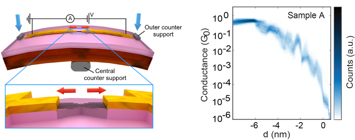
Figure 2. Schematic of the graphene mechanical break junction device (left) and electrical conductance measurements as a function of electrode displacement showing quantum mechanical interference oscillations.
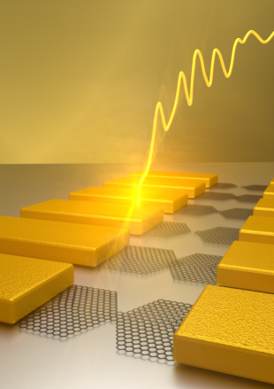
Figure 3. Artistic impression of the graphene mechanical break junction device with junction conductance signal in the background.
People working on this project


Sabina Caneva


Wayne Yang
Stephanie Heerema
Yoones Kabiri


Cees Dekker
- F0.210
- +31-(0)15-27 86094
- C.Dekker@[REMOVE THIS]tudelft.nl
- Principal Investigator
- View CV